Contact Information United States Office
12352 Sycamore Ridge Ct.
San Diego, CA 92131
Tel. : 619-857-6872
Fax. : 858-467-0215
Mobile: (619)857-6872
PCB
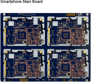
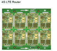
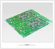
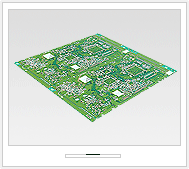
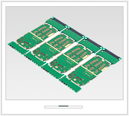
Communication and Network Products
With the continued evolution of communications development, the high-end smartphones continue cross-integration to add more features. The applications of high frequency products in PCBs have also thrived. Advancement and improvement in technology and quality are the key emphases for Dynamic in this field.
Single Side
Silver Plus Silver PCB can realize single sided CCL to have doublesided fuction. SPS PCB has V.E. effects on the single sided CCL by imaging conductor with silver paste of excellent conductivity on the non-copper side and connecting between copper side and silver conductor by STH printing method.
Carbon Plus Copper PCB can be made to have key-contact, slide switch with Carbon-Paste and Cu-Jumper with Cu-paste on a single-sided and double-side Copper Clad Laminate.Showing the multi-effects by three-dimensional pattern design.
Double Side
Silver Through Hole PCB is made with the electrical connection between both sides of the board not by copper plating but by screen printing of high conductive and reliables silver paste into the drilled hole.
Copper Paste Through Hole PCB High density C.P.T.h. PCB is made with the electrical connection between both sides of the board not by copper plating but by screen printing of high conductive and reliables silver paste into the drilled hole.
Carbon PCB can be made to have jumper, key-contact, slide switch on the single and double sided boards with carbon paste having excellent anti-abrasion, and high reliability.
PTH
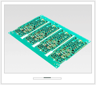
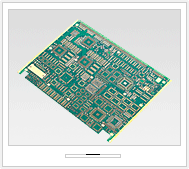
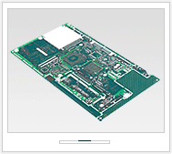
High Density PCB
PCB Density is being increased rapidly due to the introduction of new components such as BGA.CSP(Chip Size Package)or FC(Flip Chip). And, LCD related products would be also one of driven factors to accelerate density of PCBs. Moreover, growing new market fo package industry is requiring highly sophisticated PCB , which would be used as substrate for chip placing and interconnection.
Inner via Hole PCB As electronic products become highly integrated and more sophisticated, the demand for high density and size reduction of PCB is more required. Blind Via technology utilizing conventional drilling and plating make it possible ti fulfill those requirements.
Controlled Impedance PCB At high frequencies, PCB conductors can no longer be consider as simple 'piece of wire'. It is vital to control the characteristic impedance accurately to insure correct circuit operation. The faster operation speed of today's demand on PCBs with specific controlled impedance.
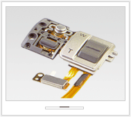
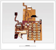
FPC
Single Side Flexible PCB The flexible printed circuit board is designed for high space efficiency and product design flexibility, which are now aiming at more compact and higher density mounting. It also contributes to the reduction of assembly process and to the enhancement of the reliability.
Double Side Flexible PCB The flexible printed circuit board is designed for high space efficiency and product design flexibility, which are now aiming at more compact and higher density mounting. It also contributes to the reduction of assembly process and to the enhancement of the reliability.
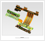
Multilayer Flexible FPC A multilayer flexible circuit is a combination of single and/or double-sided circuits bonded together and electrically interconnected by plated through holes. This technology allows high density interconnections to be achieved in applications where one or two layers of conductors could not achieve the required "pin address" or circuit packaging requirements.
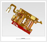
Rigid-Flex FPC Although it is similar to a multi-layer flexible circuit, a multi-layer rigid flexible circuit also utilizes rigid board inner-layer and/or outer-layer. The PWBs and FPCs are connected to each other via copper-plated through holes. It is ideal for compact, light-weight equipment design.